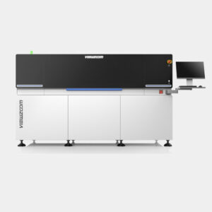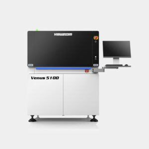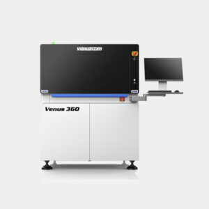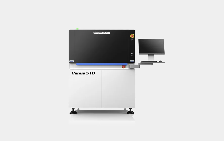

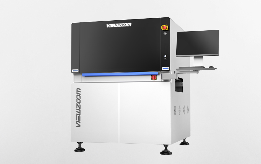
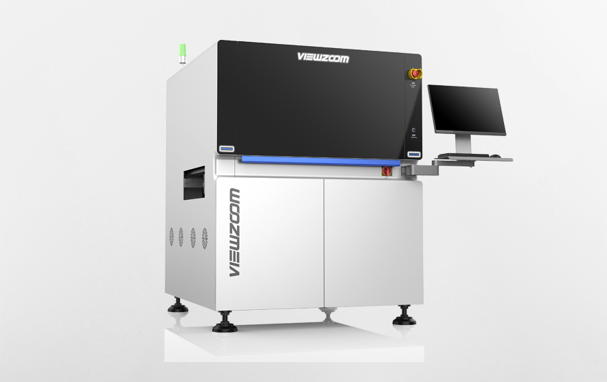
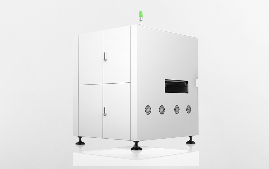
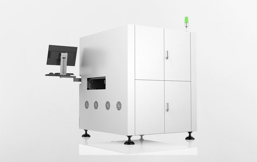
Product Overview
A 3D automated optical inspection configuration for PCB assemblies up to 510 × 510 mm. Camera resolution, component access and inspection criteria should be reviewed together to match the system to your assemblies and quality requirements.
Suitable Applications
- Post-reflow inspection of visible components and solder joints
- Assembly review using optical and height information
- PCB production requiring a 510 × 510 mm board envelope
Key Features
Match optics to the assembly
The documented standard main camera is 12 MP with 12 µm resolution. Alternative camera configurations are available. Select optics against package dimensions, surface conditions and the defects to be evaluated.
Review component and transport clearance
The listed maximum component inspection height is 35 mm, while transport clearance is 50 mm above and below the board. Transport clearance should not be treated as the validated inspection range.
Plan inspection access
An optional side camera can be discussed for accessible side views. Optical inspection requires a line of sight; hidden solder joints may require a different inspection method.
Technical Specifications
| Parameter | Documented configuration / value |
|---|---|
| PCB size range (L × W) | 50 × 50 to 510 × 510 mm |
| Maximum PCB thickness | 6 mm |
| Maximum component inspection height | 35 mm |
| Main camera | 12 MP standard; 21 MP optional |
| Camera resolution | 12 µm standard; 15 / 7 / 10 µm optional |
| Side camera | Optional |
| Transport clearance | Top 50 mm / bottom 50 mm |
| PCB bending adjustment | ±4 mm |
| Board flow | Left-to-right, right-to-left, left-to-left or right-to-right; program configuration |
| Dimensions (L × W × H) | 1100 × 1450 × 1600 mm |
| Power supply | AC 200–240 V, 50/60 Hz |
| Power consumption | 500 W standard / 800 W maximum |
| Control platform | Windows 10 listed in source documentation; confirm delivered software version |
Minimum package capability and acceptance thresholds must be evaluated for the selected optics and application; no universal defect-detection rate is implied.
Base Configuration and Options
The documented optical setup uses a 12 MP main camera and 12 µm resolution. Actual inspection capability depends on the chosen optics, programming, board geometry and acceptance criteria.
- 21 MP main-camera configuration
- 15 µm, 7 µm or 10 µm camera-resolution alternatives
- Side-camera configuration
Installation and Project Inputs
Confirm PCB support, conveyor handshakes, data outputs and available floor space. Provide representative good and defective samples for inspection programming and acceptance review. Confirm air, network and utility requirements in the installation drawing.
Product Documents
Download the three-page English selection brief with specifications, configuration choices and project preparation information.
Frequently Asked Questions
Can 3D AOI inspect every hidden BGA joint?
No. Optical inspection depends on visibility. X-ray or other methods may be needed for hidden solder joints.
Is the 50 mm clearance the inspection-height limit?
No. The product data separately lists 35 mm maximum component inspection height and 50 mm transport clearance.
Applications and Project Support
Industry Applications
Process Guides
These application routes support equipment discussion. The selected material, process or inspection task still requires a configuration review.